SiC Wafer
OST Photonics offer SiC wafers for semiconductor industry. There are two conduct types of SiC materials for you to choose from: N-type 4H-SiC...
SiC Wafer
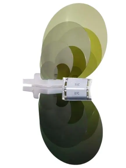
OST Photonics offer SiC wafers for semiconductor industry. There are two conduct types of SiC materials for you to choose from: N-type 4H-SiC (Conductivity Type) and high purity semi-insulating (HPSI) 4H-SiC. High purity semi-insulating SiC wafers is mainly used in 5G communication applications. It has the advantages of improving the radio frequency range, ultra-long distance recognition, anti-interference, high-spee...
- ManufacturerOST Photonics
- CategoryCrystal Wafer and Substrate
- Lead TimeQuoted per order
- CustomizationSize, orientation and surface finish to drawing
OST Photonics offer SiC wafers for semiconductor industry. There are two conduct types of SiC materials for you to choose from: N-type 4H-SiC (Conductivity Type) and high purity semi-insulating (HPSI) 4H-SiC. High purity semi-insulating SiC wafers is mainly used in 5G communication applications. It has the advantages of improving the radio frequency range, ultra-long distance recognition, anti-interference, high-speed and large-capacity information transmission, and is regarded as the most ideal material for making microwave power devices. N-type SiC wafer is mainly used in new energy vehicles, high voltage transmission and transformation stations, white goods, high-speed trains, motors, photovoltaic inverter, pulse power supply and other fields, it has the advantages of reducing equipment energy loss, improving equipment reliability, reducing equipment volume, improving equipment performance and so on, it has irreplaceable advantages in the production of power electronic devices.
Specifications of N-type 4H-SiC Wafers (Conductivity Type)
| N-type 4H-SiC Wafers (Conductivity Type) | ||||
| Diameter | 2”-50 .8 mm | 4″- 100.0 mm | 6″- 150.0 mm | 8”-200.0 mm |
| Thickness | 350μm(DSP) | 500μm(DSP) | ||
| Surface Orientation | Off-Axis:<0001> 4 ° toward <11- 20> ± 0 . 5° | |||
| Primary Flat Orientation | Parallel to <1 1 -20 > ±1 ° | < 1-100> ± 1 ° | ||
| Primary Flat Length | 16.0 mm | 32 . 5 mm | 47.5mm | Notch |
| Secondary Flat Orientation | Silicon face up: 90.0 ˚ CW from Primary ± 5.0˚ | N/A | N/A | |
| Secondary Flat Length | N/A | 18.0 mm | N/A | N/A |
| Resistivity | 0 . 014 ~ 0 . 028 Ω . cm | |||
| Front Surface | Si-Face : CMP , Ra<0 . 2nm | |||
| Back Surface | C-Face : optical polish, Ra<0 . 5nm | |||
| Laser Marking | Back side : C-Face | |||
| TTV | ≤ 10 μm | ≤ 15 μm | ≤ 15 μm | ≤ 20 μm |
| BOW | ≤ 25 μm | ≤ 30μm | ≤40 μm | ≤ 60μm |
| WARP | ≤ 30μm | ≤ 40 μm | ≤ 60μm | ≤ 80μm |
| Edge Excluding | ≤ 3 mm |
Specifications of High Purity Semi-insulating (HPSI) 4H-SiC Wafers
| High Purity Semi-insulating (HPSI) 4H-SiC Wafers | |||||
| Diameter | 2”- 50 .8mm | 3”- 76.2 mm | 4”- 100mm | 6”-150mm | 8”-200mm |
| Thickness | 500μ m (DSP) | ||||
| Surface Orientation | <0001> ± 0 . 25 ° | ||||
| Primary Flat Orientation | < 1- 100 > ±1° | ||||
| Primary Flat Length | 16.0 mm | 22.0mm | 32 .5mm | Notch | Notch |
| Secondary Flat Orientation | Silicon face up: 90.0 ˚ CW from Primary ± 5.0˚ | N/A | N/A | ||
| Secondary Flat Length | 8mm | 11mm | 18 mm | N/A | N/A |
| Resistivity | > 1 E7 Ω .cm | ||||
| Front Surface | Si- Face: CMP, Ra<0 . 2nm | ||||
| Back Surface | C-Face:CMP,Ra<0.2nm | C-Facepolished.Ra<5nm | |||
| Laser Marking | Back side: C-Face | ||||
| TTV | ≤10 μm | ≤15 μm | ≤15 μm | ≤15 μm | ≤20 μm |
| BOW | ≤25 μm | ≤25 μm | ≤30μm | ≤45 μm | ≤ 65μm |
| WARP | ≤ 30μm | ≤35μm | ≤40 μm | ≤60μm | ≤70 μm |
| Edge Excluding | ≤ 3 mm |
Specifications of Special Polytype SiC Wafers
| Special Polytype SiC Wafers (6H-N/4H-P/6H-P/3C-N) | |||
| Dimensions | 10 * 10 mm | 2”- 50 .8mm | 4”- 100mm |
| Thickness | 350μm(DSP) | ||
| Polytype | 6H/4H-P/6 H-P/3C-N | ||
| Surface Orientation (6H-N/4H-P/6H-P) | Off Axis: 0 . 0 °- 8 . 0 °toward < 11 – 20 > ± 0 . 5° | ||
| Surface Orientation (3C-N) | On axis : <0001 > ± 0 . 5 ° | ||
| Resistivity (6H-N/4H-P/6H-P) | ≤ 0 . 5 Ω · cm | ||
| Resistivity (3C-N) | ≤ 1 . 0 mΩ · cm | ||
| Front Surface | Si- Face: CMP, Ra<0 . 5nm | ||
| Back Surface | C-Face: ptical polish, Ra< 1 .0 nm | ||
| Laser Marking | Back side : C- Face | ||
| TTV | ≤ 5 μ m | ≤ 10 μ m | ≤ 15 μ m |
| BOW | ≤ 15 μ m | ≤ 25 μ m | ≤ 25 μm |
| WARP | ≤ 30μ m | ≤ 30μ m | ≤ 40 μ m |
Specifications of High Purity Semi-insulating (HPSI) 4H-SiC Ultra-thin Wafers
| HPSI 4H-SiC Ultra-thin Wafer | |||
| Diameter | 2”- 50 .8mm | 4”- 100mm | 6”- 150mm |
| Dimensions | 50.8*50.8mm/76.2*76.2mm/100*100mm | ||
| Thickness | 150μ m /200μ m /250μ m /350μ m | ||
| Surface Orientation | {0001} ± 0 . 25 ° | ||
| Primary Flat Orientation | < 1- 100> ±1° | ||
| Primary Flat Length | 16.0 mm | 32 .5mm | Notch |
| Secondary Flat Orientation | Silicon face up: 90.0 ˚ CW from Primary ± 5.0˚ | N/A | |
| Secondary Flat Length | 8mm | 18 mm | N/A |
| Resistivity | > 1 E7 Ω .cm | ||
| Surface finish | Polished, Ra≤ 10nm | Ultrathin, Ra<20nm | |
| Laser Marking | Back side: C-Face | ||
| TTV | ≤15 μm | ≤20 μm | ≤30μm |
| Edge Excluding | ≤ 3 mm |
Properties of SiC Single Crystal
| Silicon Carbide Single Crystal | |
| Crystal Structure | Hexagonal Crystal |
| Band gap (eV) | 3 .26 eV |
| Melting Point (℃) | 2730 ℃ |
| Mohs Hardness (mohs) | 9.2 |
| Heat Conductivity (W·cm^-1· ℃^-1) | 4. 9 W·cm^-1· ℃^-1 |
| Coefficient of Thermal Expansion (℃^-1) | 4.7 x 10^-6 |
| Lattice Constant (nm) | a =0 .3076 c = 0 .5048 |
| Electronic Mobility (cm^-2.V^-1.s^-1) | 720^a 650^c |
| Disruptive Field (MV· cm^-1) | 3.1 |
| JFM Index (power) | 410 |
| BFM Index (SW) | 290 |
| BHFM Index (RF) | 34 |
| Refractive Index | 2.6767 ~ 2.6480 |
Other Crystal Wafer and Substrate Materials
Request A Quote For SiC Wafer
Send us your dimensions, orientation, surface finish and quantity. Our engineers reply with a technical proposal and price.
Buyer Questions
What is the surface orientation of the SiC Wafer?
What is the resistivity of the SiC Wafer?
What is the front surface of the SiC Wafer?
What is the back surface of the SiC Wafer?
How do I get a quotation for the SiC Wafer?
Can the SiC Wafer be made to a custom specification?
Who manufactures the SiC Wafer?
Tell Us What You Need
Send your specification, quantity and destination port. Our engineers reply with a technical proposal and a confirmed lead time.