Silicon Substrate
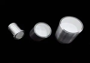
Silicon single crystals are used as a semiconductor material, high-power transistor, rectifier, solar cells, etc. OST Photonics offers high quality...
Silicon Substrate
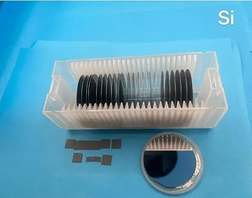
Silicon single crystals are used as a semiconductor material, high-power transistor, rectifier, solar cells, etc. OST Photonics offers high quality Silicon substrates for researchers and industries. Crystal orientation, size and thickness can be customized according to your requirements.
- ManufacturerOST Photonics
- CategoryCrystal Wafer and Substrate
- Lead TimeQuoted per order
- CustomizationSize, orientation and surface finish to drawing
Features
- Low cost
- Safe and non-toxic
- Excellent machinability
- Large size available
Applications
- Integrated circuits
- Semiconductor device
- Consumer electronics
- Solar cell substrate
Processing Capability
- Orientation: <100>,<111>,<110>, etc.
- Dimension: 2”, 3”, 4”, 5”, 6”, 8”, 12”, 5x5mm, 10x10mm, 20x20mm etc.
- Thickness: 279 μm, 380 μm, 525 μm, 625 μm, 675 μm, 725 μm, 775 μm, 500 μm, 1000 μm etc.
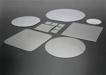
- Available items: wafers, substrates, blanks and customized optics
Specification and Properties of Silicon Substrates
| Crystal Structure | Cubic | ||
| Melting Point | 1420 ℃ | ||
| Density | 2.4 g/cm3 | ||
| Dopant | Undoped | Boron | Phosphorus |
| Conduction type | Intrinsic | P-type | N-type |
| Resistivity | >1000 ohm.cm | 0.001~1000 ohm.cm | 0.001~1000 ohm.cm |
| EPD | ≤100 ∕cm2 | ≤100 ∕cm2 | ≤100 ∕cm2 |
| Oxygen content(∕cm3) | ≤1~1.8×10^18 | ≤1~1.8×10^18 | ≤1~1.8×10^18 |
| Carbon content(∕cm3) | ≤5×10^16 | ≤5×10^16 | ≤5×10^16 |
| Orientation | <100>,<111>,<110>, etc. | ||
| Orientation Tolerance | ±0.5° or better | ||
| Dimension | 2”, 3”, 4”, 5”, 6”, 8”, 12”, 5x5mm, 10x10mm, 20x20mm etc. | ||
| Dimension Tolerance | ±0.1 mm or better | ||
| Thickness | 279 μm, 380 μm, 525 μm, 625 μm, 675 μm, 725 μm, 775 μm, 500 μm, 1000 μm etc. | ||
| Thickness Tolerance | ±0.025 mm or better | ||
| Surface Finish | Single side polished (SSP)/Double sides polished (DSP) | ||
| Package | Class 100 clean bag, Class 1000 super clean room |
Other Crystal Wafer and Substrate Materials
Request A Quote For Silicon Substrate
Send us your dimensions, orientation, surface finish and quantity. Our engineers reply with a technical proposal and price.
FAQ
Buyer Questions
What is the crystal structure of the Silicon Substrate?
The crystal structure of the Silicon Substrate is Cubic.
What is the melting point of the Silicon Substrate?
The melting point of the Silicon Substrate is 1420 ℃.
What is the density of the Silicon Substrate?
The density of the Silicon Substrate is 2.4 g/cm3.
What is the orientation of the Silicon Substrate?
The orientation of the Silicon Substrate is <100>,<111>,<110>, etc..
How do I get a quotation for the Silicon Substrate?
Send the quantity, the specification and your destination port to Jiaxing AOSITE Photonics Technology Co.,Ltd. by email or telephone. There is no enquiry form on this site, so your message reaches an engineer directly rather than a contact queue.
Can the Silicon Substrate be made to a custom specification?
Custom dimensions and finishes are quoted case by case against your drawing or written specification. Send what you need and the factory will confirm what is achievable, and at what tolerance, before you place the order.
Who manufactures the Silicon Substrate?
Jiaxing AOSITE Photonics Technology Co.,Ltd., trading as OST Photonics, manufacturing in Jiaxing, Zhejiang, China since 2010.
Tell Us What You Need
Send your specification, quantity and destination port. Our engineers reply with a technical proposal and a confirmed lead time.