

ZnSe Substrate
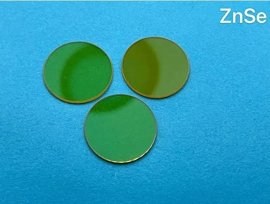
Zinc selenide (ZnSe) crystal substrate is widely used in the field of infrared optics, lens, window, beam splitter, epitaxial substrate, evaporation...
ZnSe Substrate
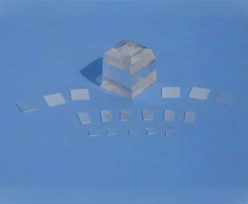
Zinc selenide (ZnSe) crystal substrate is widely used in the field of infrared optics, lens, window, beam splitter, epitaxial substrate, evaporation source crystal and so on. OST Photonics offers high quality ZnSe substrates for researchers and industries. Crystal orientation, size and thickness can be customized according to your requirements.
- ManufacturerOST Photonics
- CategoryCrystal Wafer and Substrate
- Lead TimeQuoted per order
- CustomizationSize, orientation and surface finish to drawing
Features
- Low optical transmission loss
- Good light transmission performance
- Uniform refractive index
- Good consistency
Applications
- Thermal imaging system
- Epitaxial substrate
- Infrared spectrometer
- Thermal radiation measuring instrument
- Laser optical element
Processing Capability
- Orientation: <100>, <110>, <111>, etc.
- Dimension: 1”, 2”, 5x5mm, 10x5mm, 10x10mm, etc.
- Thickness: 0.5mm, 1.0mm, 2mm, 5mm, etc.
- Available items: wafers, substrates, blanks and customized optics
Specification and Properties of ZnSe Substrates
| Crystal System | Cubic |
| Growth Method | PVT |
| Crystal Lattice Constant | a=5.6685 Å |
| Purity | 99.95% |
| Density | 5.264 g/cm3 |
| Dielectric Constant | 8.976 |
| Thermal Expansion Coefficient | 7.1 ppm/℃ |
| Refractive Index | 2.5 |
| Orientation | <100>,<110>,<111>, etc. |
| Orientation Tolerance | ±0.5° or better |
| Dimension | 1”, 2”, 5x5mm, 10x5mm, 10x10mm, etc. |
| Dimension Tolerance | ±0.1 mm or better |
| Thickness | 0.5mm, 1.0mm, 2mm, 5mm, etc. |
| Thickness Tolerance | ±0.05 mm or better |
| Surface Finish | Single side polished (SSP)/Double sides polished (DSP) |
| Surface Roughness | Ra<5Å (5µmx5µm) |
| Package | Class 100 clean bag, Class 1000 super clean room |
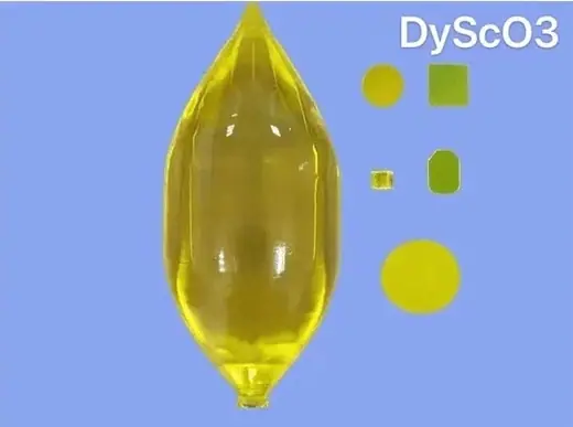
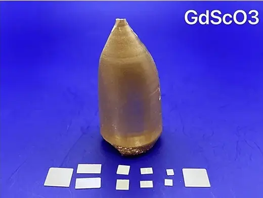
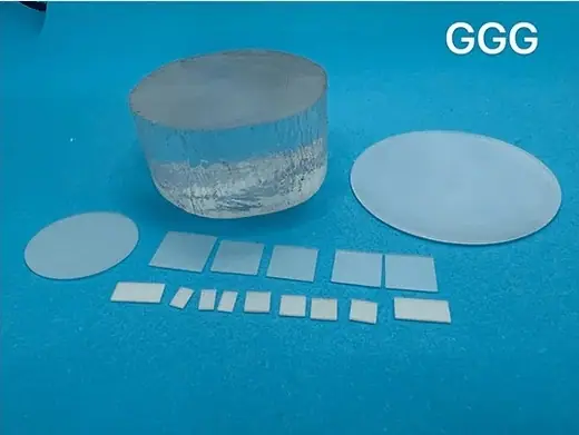
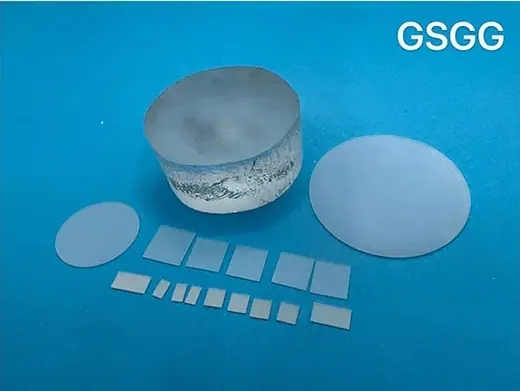
Other Crystal Wafer and Substrate Materials
Request A Quote For ZnSe Substrate
Send us your dimensions, orientation, surface finish and quantity. Our engineers reply with a technical proposal and price.
FAQ
Buyer Questions
What is the crystal system of the ZnSe Substrate?
The crystal system of the ZnSe Substrate is Cubic.
What is the growth method of the ZnSe Substrate?
The growth method of the ZnSe Substrate is PVT.
What is the crystal lattice constant of the ZnSe Substrate?
The crystal lattice constant of the ZnSe Substrate is a=5.6685 Å.
What is the purity of the ZnSe Substrate?
The purity of the ZnSe Substrate is 99.95%.
How do I get a quotation for the ZnSe Substrate?
Send the quantity, the specification and your destination port to Jiaxing AOSITE Photonics Technology Co.,Ltd. by email or telephone. There is no enquiry form on this site, so your message reaches an engineer directly rather than a contact queue.
Can the ZnSe Substrate be made to a custom specification?
Custom dimensions and finishes are quoted case by case against your drawing or written specification. Send what you need and the factory will confirm what is achievable, and at what tolerance, before you place the order.
Who manufactures the ZnSe Substrate?
Jiaxing AOSITE Photonics Technology Co.,Ltd., trading as OST Photonics, manufacturing in Jiaxing, Zhejiang, China since 2010.
Tell Us What You Need
Send your specification, quantity and destination port. Our engineers reply with a technical proposal and a confirmed lead time.